Table Of Content

Circuit designers, PCB layout engineers, and simulation engineers trust the complete set of circuit board design tools in Altium Designer®. When a circuit board design is finished and ready to be released to manufacturing, the Altium 365™ platform makes it easy to collaborate and share your projects. The functionality and capabilities discussed here only scratch the surface of what is available to you.
WHY CHOOSE ADVANCED CIRCUITS, INC. (ACI)?
The interactive routing tools allow you to route PCB layouts from any angle at fast speeds, while the Layer Stackup feature helps to reduce noise and improve signal timing even on highly complex circuit boards. Altium Designer’s unified environment provides includes everything needed to design and manufacture high-quality printed circuit board assemblies. Other programs separate your important design tools into different programs with different workflows, making it difficult to stay productive and increasing your licensing costs. Altium Designer is consistently rated as the easiest to learn and the easiest to use, making it ideal for new designers and experienced professionals. If you want to easily get through all of these stages in the PCB electronics board design process, you need to use the best design software with an intuitive user interface and a complete set of PCB design features.
Ensure a Clear PCB Return Current Path
Each outer connection on the die is connected via a tiny piece of gold wire to a pad or pin on the package. Pins are the silver, extruding terminals on an IC, which go on to connect to other parts of a circuit. These are of utmost importance to us, because they're what will go on to connect to the rest of the components and wires in a circuit.
Use Altium Designer to Create Your Printed Circuit Boards
As such, they can save time and money, making these tools an essential part of the PCB design process. They are all designed to sit on one side of a circuit board and be soldered to the surface. The pins of a SMD package either extrude out the side, perpendicular to the chip, or are sometimes arranged in a matrix on the bottom of the chip. ICs in this form factor are not very "hand-assembly-friendly." They usually require special tools to aid in the process.
Easy-to-use & Free PCB Design Software
Using net names is also helpful once you're in the PCB layout as you'll be able to quickly identify nets during placement and routing. This will also help once you go to test your finished prototype as you'll be able to quickly track nets in the corresponding PCB layout in Altium Designer. You need to transfer your schematic diagram into a drawing of your printed circuit board. This tutorial will breakdown what makes up a PCB and some of the common terms used in the PCB world. In the other case, where the pinouts and/or packages do not match, it’s difficult to generalize a routing strategy.
Carrier boards are not typically used in production, and I would argue they should not be used in this way. Instead, they are prototyping tools that allow you to get a PCB assembly completed without having to scrap your set of bare boards. Sometimes, footprints end up being incorrect, and they simply aren’t caught in a design review. In addition, some components do not have a replacement part in a matching footprint, and any other available components might not match the pinout on the device. If you follow points #1 and #2, it's much easier to lay out the rest of your board without too much crossover between routes. In addition, your board will have that modern look and feel to the layout, where a central processor supplies data to all the other components around the perimeter of a board.
Renesas to acquire PCB design software provider Altium - New Electronics
Renesas to acquire PCB design software provider Altium.
Posted: Thu, 15 Feb 2024 08:00:00 GMT [source]
Circuit board parts have been traditionally difficult to find, and many designers have spent hours creating these parts manually. Altium Designer offers access to a Manufacturer Part Search panel, which helps you quickly add components to your library. All you have to do is search and click to download accurate parts directly from a managed library. Forget about learning through trial and error, your PCB design software should guide you through the basic design tools and introduce you to advanced features that maximize productivity.
One of the great things about PADS is that it offers several different solutions to suit teams with different budgets and experience levels. For starters there’s PADS Standard, which starts at $5,000 (including support) and provides the core schematic and PCB layout tools in an intuitive environment. Another of the best circuit design software is PADS, developed by Siemens Digital Industries Software. CircuitMaker is a free and easy PCB design software developed by Altium, which also provides some of the top industrial PCB software (more on that later). While Upverter is an ideal starting point for students and beginners, it lacks the advanced functionality of other options.
When inexpensive computer processing became available in the 1970s, computer programs were written to simulate circuit designs with greater accuracy than practical by hand calculation. The first circuit simulator for analog ICs was called SPICE (Simulation Program with Integrated Circuits Emphasis). Computerized circuit simulation tools enable greater IC design complexity than hand calculations can achieve, making the design of analog ASICs practical. Today, standard designs can have many small components, such as tiny ICs, very small passive components, and advanced chips with very high pin counts.
The small feature sizes used in UHDI PCBs are pushing the limits of many manufacturers, and currently these capabilities are only accessible at scale in Taiwan. However, global UHDI capacity is increasing due to significant investment by Western nations. These PCBs will also be the main drivers of the most advanced systems operating at the highest data rates. Although the production processes are very different, the process for designing UHDI PCBs is very similar to that for conventional PCBs. The main component packaging type that can drive the use of HDI design and manufacturing in a PCB build is ball grid array (BGA) packaging, as well as related packaging types like land grid array (LGA).
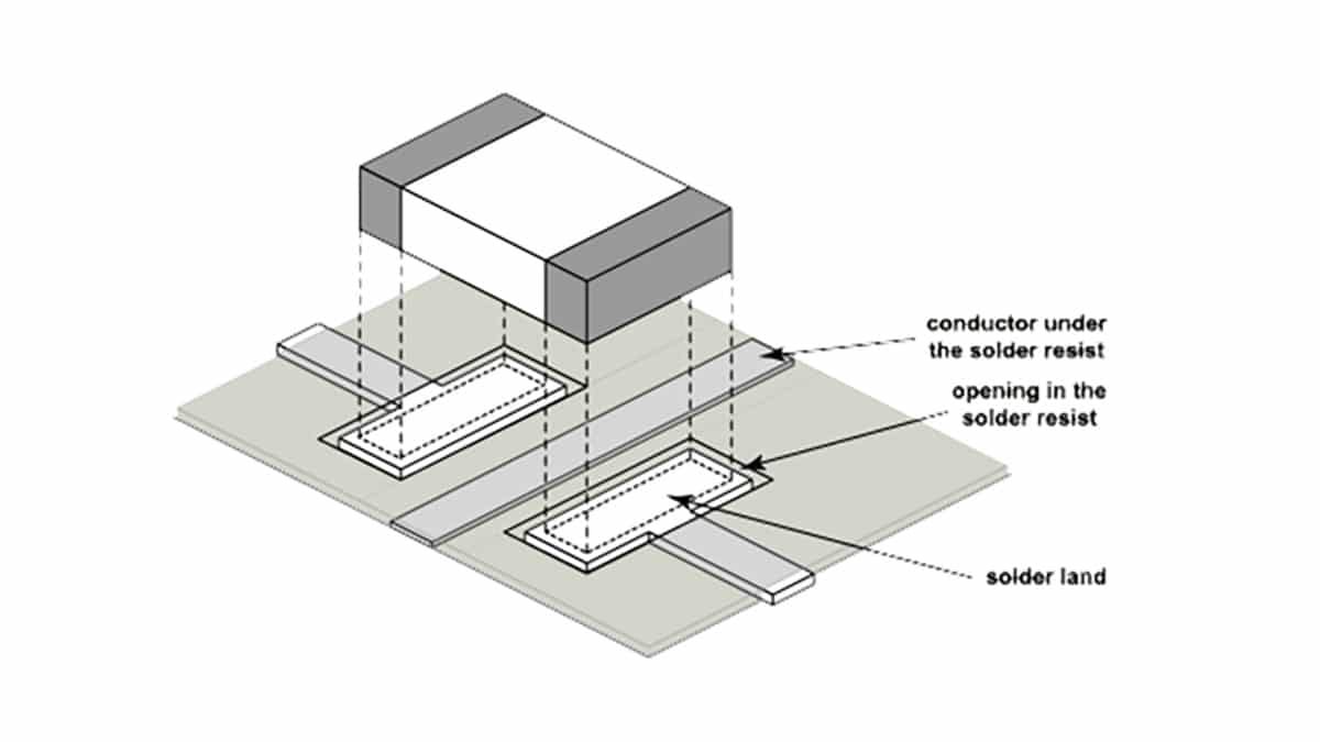
There are many different types of packages, each of which has unique dimensions, mounting-types, and/or pin-counts. To design a Printed Circuit Board (PCB), you need to draw holes, pads, and wires for your circuit. It is overlaid onto the copper layer to insulate the copper traces from accidental contact with other metal, solder, or conductive bits.


No comments:
Post a Comment